打包
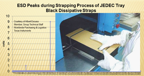
我們提供最高質量,最經濟實惠的靜電屏蔽包裝。透明度為40%,便於識別IC(集成電路)和PCB(印刷電路板)。極其耐用的埋地金屬結構提供了有效屏蔽這些部件免受靜電損耗所需的FaradayCage性能。
所有產品都將包裝在防靜電袋中。裝有ESD防靜電保護裝置。
外部ESD包裝的標籤將使用我們公司的信息:零件Mumber,品牌和數量。
我們會在發貨前檢查所有貨物,確保所有產品都處於良好狀態,並確保零件是新的原始數據表。
所有貨物在包裝後確保沒有問題,我們將安全包裝並通過全球快遞發送。它具有優異的抗穿刺和抗撕裂性以及良好的密封完整性。
我們可以提供全球快遞服務,如DHLor FedEx或TNT或UPS或其他貨運代理商。

DHL / FedEx / TNT / UPS全球發貨
運費參考DHL / FedEx
1)。您可以提供快遞賬單以便裝運,如果您沒有任何快遞賬單,我們可以提供我們的賬戶。
2)。使用我們的帳戶進行裝運,裝運費用(參考DHL / FedEx,不同國家有不同的價格。)
| 裝運費用: |
(參考DHL和FedEX) |
| 重量(KG):0.00kg-1.00kg |
價格(美元):60.00美元 |
| 重量(KG):1.00kg-2.00kg |
價格(美元):80.00美元 |
*成本價格參考DHL / FedEx。詳細收費,請聯繫我們。不同國家的快遞費用不同。
- 其他裝運方式: 順豐速運亞洲; Chang-woo為韓國特殊航線,Aramexfor中東國家。其他更多的運輸方式,請與我們聯繫。
我們也可以將貨物發送給您的貨運代理或其他供應商,以便您可以將貨物一起發送。它可能會為您節省運費,或者可能更方便您。
- 送貨細節: 運輸信息,我們需要運輸信息,包括收貨人公司名稱(或個人),收貨人姓名,聯繫電話,地址和郵政編碼。請確保這些信息給我們,以便我們更快地安排發貨。
- 交貨時間: 對於DHL / UPS / FEDEX / TNT,交付時間需要2-5天到全世界大部分國家。
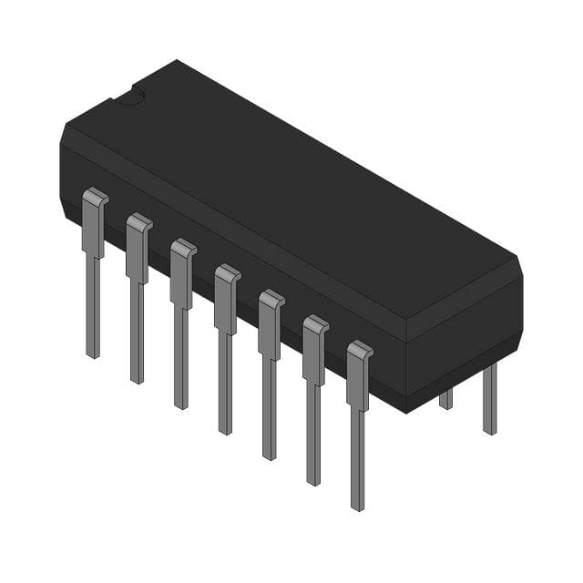
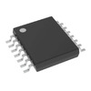
CD4011UBF 產品詳情:
"CD4011UBF Integrated Circuit (IC): A Comprehensive Guide to Its Features, Scenarios, and Performance Parameters"
Are you looking for a high-performance integrated circuit for your electronic device or industrial application? Look no further than the CD4011UBF. This specialized Hot IC is a CD4011UB-MIL CMOS QUAD 2-INPUT N integrated circuit that is designed to deliver unparalleled performance and efficiency. In this article, we will provide you with essential information about the CD4011UBF, including its features, application scenarios, usage, and performance parameters.
Main Features:
The CD4011UBF boasts an array of features that make it an ideal choice for demanding applications. Its key features include:
- Quad 2-Input N gate
- Wide supply voltage range: 3V to 18V
- Low power consumption
- High noise immunity
- TTL-compatible
- MIL-STD-883 compliant
Product Classification:
The CD4011UBF belongs to the family of digital integrated circuits (ICs). This type of IC uses digital signals to process and transmit information, making it a powerful tool for electronic devices and systems.
Application Scenarios and Usage:
The CD4011UBF can be used for a wide range of electronic devices and industries. This includes applications in aerospace, defense, automotive, medical, and consumer electronics. It can be used in various specific applications such as signal processing, data storage, motor control, and power management. Its robustness and MIL-STD-883 compliance make it a reliable choice in harsh environments.
Performance Parameters:
The CD4011UBF has outstanding performance parameters that set it apart from other integrated circuits. Its output voltage can range from 0V to VDD, and its maximum output current is 6mA. Its power consumption is as low as 5uA, and it has a temperature range of -55°C to 125°C. These parameters make it a highly accurate and precise integrated circuit that operates efficiently and consistently.
Types of Integrated Circuits:
Integrated circuits come in different variants, including digital, analog, mixed signal, and RF. Digital integrated circuits like CD4011UBF use binary data to process and transmit information. Analog integrated circuits, on the other hand, use continuous signals. Mixed-signal integrated circuits combine both digital and analog circuits. RF (Radio frequency) integrated circuits are designed for wireless communication systems.
Manufacturing Process:
Integrated circuit manufacturing is a complex process that requires precision and sophistication. The manufacturing process includes chip design, cutting, cleaning, laser processing, back grinding, doping, exposure, vapor deposition, etching, and more. Chip design is the initial process where designers select the materials and layout of circuits. Cutting and cleaning involve filtering and cleaning impurities. Laser processing is used to create circuit patterns on the wafer. Doping and exposure create the transistors and interconnections, while vapor deposition and etching create the conductive layers.
Packaging and Testing:
Finished integrated circuits need to undergo appropriate packaging and testing to ensure component quality. Packaging involves placing the integrated circuit in a protective casing, ensuring that it will operate under varying temperature, humidity, and mechanical stresses. Testing ensures that the integrated circuit meets the specified parameters and technical specifications.
Conclusion:
The CD4011UBF integrated circuit is an exceptional component with superior features, performance parameters, and robustness. Its MIL-STD-883 compliance makes it a reliable choice for defense and aerospace applications. It's a versatile component that can be used in various electronic devices and industries. This article sheds light on the manufacturing process, types of integrated circuits, and how to ensure quality through packaging and testing. Make the CD4011UBF your integrated circuit of choice for your next project, and you're guaranteed of high efficiency and excellent performance.