포장
우리는 최고 품질의 경제적 인 가격의 정적 차폐 포장을 제공합니다. 40 %의 빛 투과율로 IC (집적 회로) 및 PCB (인쇄 회로 기판)를 쉽게 식별 할 수 있습니다. 매우 내구성있는 매장 금속 장식으로 정전기를 효과적으로 차단하는 데 필요한 FaradayCage 성능을 제공합니다.
모든 제품은 정전기 방지 백으로 포장됩니다. ESD 정전기 방지 보호 장치와 함께 제공하십시오.
외부 ESD 포장의 lable은 부품 회사의 정보 (부품 수, 브랜드 및 수량)를 사용합니다.
우리는 선적 전에 모든 물품을 검사하고 모든 제품을 양호한 상태로 유지하며 부품이 새로운 원본 조달 데이터 시트인지 확인합니다.
모든 제품이 포장 후 문제가 없는지 확인한 후, 우리는 안전하게 포장하고 글로벌 익스프레스로 보낼 것입니다. 그것은 밀봉 성이 양호하고 꿰 뚫음 저항성이 우수합니다.
DHL 또는 FedEx 또는 TNT 또는 UPS 또는 선적을위한 다른 운송 업체와 같은 전세계 특송 서비스를 제공 할 수 있습니다.

DHL / FedEx / TNT / UPS의 글로벌 발송
배송비 참조 DHL / FedEx
1). 배송을위한 특송 계정이 없다면 신속한 배송 계정을 제공 할 수 있습니다.
2). 발송물, 발송 비용 (참조 DHL / FedEx, 국가마다 가격이 다릅니다.)
| 배송료 : |
(참조 DHL 및 FedEX) |
| 무게 (KG) : 0.00kg-1.00kg |
가격 (USD $) : USD $ 60.00 |
| 무게 (KG) : 1.00kg-2.00kg |
가격 (USD $) : USD $ 80.00 |
* 비용은 DHL / FedEx를 참조하십시오. 세부 요금은 문의하십시오. 특급 요금이 다른 나라.
- 기타 선적 방법 : SF Express for Asia; 창 - 우 특수선, 한국 Aramex for 중동 국가 기타 배송 방법이 더 있으시면 연락주십시오.
우리는 또한 물건을 함께 보낼 수 있도록 전달자 또는 다른 사람에게 물품을 보낼 수 있습니다. 배송료를 절약 할 수 있거나 더 편리 할 수 있습니다.
- 배송 정보: Shippinginformation, 우리는 운송 회사 이름 (또는 개인), 수신자 이름, 연락처 번호, 주소 및 우편 번호를 포함한 운송 정보가 필요합니다. 우리가 선적을 더 빨리 처리 할 수 있도록이 정보를 저희에게 알려주십시오.
- 배달 시간: 배달 시간은 DHL / UPS / FEDEX / TNT를 위해 전세계 대부분의 국가에 2 ~ 5 일이 필요합니다.
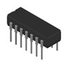
CD4012BM 제품 상세 정보:
CD4012BM Integrated Circuits (ICs): A Comprehensive Guide to Logic Gates and Inverters
Integrated circuits are a core component of modern electronics, and they serve as the building blocks of most electronic devices. One such integrated circuit is the CD4012BM, a digital NAND gate designed for various electronic applications. In this article, we will explore the main features, performance parameters, application scenarios, and usage of the CD4012BM.
Product Model and Main Features
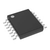
The CD4012BM is a digital integrated circuit that contains two nand gates with a total of 4 inputs. It operates with a wide range of input voltages, from 3 volts to 18 volts DC, and has a temperature range of -55°C to 125°C. This integrated circuit is manufactured in CMOS technology, making it a reliable and energy-efficient solution. It is available in a surface-mount device (SMD) package and has 14 leads (SO14).
Product Classification and Application Scenarios
The CD4012BM is part of the Logic - Gates and Inverters category, which contains other similar ICs. It is often used in the design of microprocessors and digital circuits that require NAND gates. This IC is commonly utilized in different applications such as motor control, signal processing, and power management. It can also be used as a building block for more complex digital circuits.
Usage and Performance Parameters
The CD4012BM is an ideal solution for designers where digital logic is required and an inverted output is necessary. With its high switching speed and low power consumption, it is suitable for portable and battery-powered devices. Its high accuracy and efficiency make it an excellent choice for precise digital control systems. The CD4012BM has a maximum output current of 6mA, a supply current of 0.4uA, and a propagation delay of 55ns. All these performance parameters make it more versatile and reliable than its competitors.
Different Types of Integrated Circuits
Integrated circuits are grouped based on their functionality and mode of operation. Digital ICs, including the CD4012BM, operate on binary logic and are used in computers, memory systems, and digital signal processing. Analog ICs work on continuous signals and find their use in amplifiers, voltage regulators, and audio or video circuits. Mixed-signal ICs combine both analog and digital circuits and are used in applications where both are required. Finally, RF ICs are used to amplify, filter, and modulate high-frequency signals in mobile communication systems and radar applications.
Manufacturing Process and Package Testing
The creation of an integrated circuit is a complex process that involves various steps like design, simulation, layout, fabrication, testing, and packaging. The manufacturing process of ICs includes chip design, cutting, cleaning, laser processing, back grinding, doping, exposure, vapor deposition, etching, photolithography, and more. The finished products undergo appropriate testing to ensure consistent quality. The IC is packaged and tested to ensure the highest level of reliability, performance, and durability.
Conclusion
The CD4012BM is a highly reliable and versatile digital NAND gate that can be used in a wide variety of electronic devices and applications. With its fast switching speeds, low power consumption, and wide input voltage range, it is capable of meeting the demands of various digital control and switching systems. We hope this article has helped you understand the features, performance parameters, application scenarios, and manufacturing process of the CD4012BM IC.